Tekscend Photomask Japan Launches its new Nanoimprint Lithography line (NIL) Capabilities
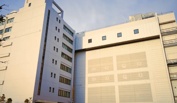
Tekscend Photomask Corp. (Headquarters: Minato-ku, Tokyo; Representative Director, President & CEO: Teruo Ninomiya; "Tekscend Photomask" below) has kicked off development of nanoimprint lithography (NIL) capabilities at its Asaka site (Niiza City, Saitama) to support next-generation optical components2 for applications such as AR/MR devices. The facility, equipped with EV Group’s state-of-the-art HERCULES® NIL 200mm system, will enable domestic prototyping towards production starting September 2025.
Traditionally, optical components such as light-guide mold designs, which are essential for AR/MR devices, have relied on complex photolithography and etching processes for prototyping and production optimization. These methods often present challenges related to cost, efficiency, and scalability when transitioning to volume production. Tekscend Photomask addresses these challenges by leveraging its semiconductor photomask expertise to build advanced nanoimprint lithography (NIL) mold capabilities. This vertically integrated platform streamlines workflows for customers and offers a comprehensive solution that includes in-house design simulations, mold fabrication, prototyping, and volume production2.
NIL technology is increasingly recognized as a key enabler for next-generation lower cost optical elements, including Meta-Surfaces and other advanced nano structure components. Its ability to replicate high-precision nanometer-scale patterns in a single imprint step consolidates complex processes, significantly improving scalability and reducing costs. These advantages place NIL as a critical technology for supporting emerging applications in AR/MR and other advanced optics markets.
Key Features of Tekscend’s NIL Manufacturing Services
・Cutting Edge NIL System
Tekscend Photomask will be introducing the EV Group HERCULES® NIL 200mm, a fully integrated nanoimprint lithography system allowing Tekscend Photomask to become the first merchant mask shop to offer this capability. The system supports replication for substrate sizes from 100mm to 200mm (round) for small-scale prototyping to high-volume production.
・Advanced Cleanroom Environment
With the introduction of its new nanoimprint lithography manufacturing line Tekscend Photomask has built a cleanroom environment on par with its semiconductor photomask manufacturing lines for defect control and high-quality replica products from prototyping, optimization, and volume production.
・In-House Mold Production
Tekscend Photomask will support produce silicon master molds up to φ200mm, enabling customers to develop large-area nanoimprint products for small-volume production. The company also offers six-inch square quartz molds fabricated from semiconductor photomask blanks.

The "HERCULES® NIL 200mm" nanoimprint lithography system manufactured by the EV Groupⓒ EV Group
*1: Refers to "nanoimprinting."
*2: Microfabrication technology in which molds serving as the original plates are stamped in order to transfer patterns in the order of several nanometers.
About Tekscend Photomask
Tekscend Photomask Corp. is the world’s premier provider of photomasks for semiconductors and a group company of TOPPAN Holdings Inc. (TYO: 7911). Tekscend Photomask was previously known as Toppan Photomask. Headquartered in Tokyo, Tekscend Photomask leverages its worldwide customer service network and eight manufacturing facilities in key geographic locations to offer the world's most advanced lithography technology. Tekscend Photomask is also expanding into nanoimprint molds and other nano-fabricated products. For more information, visit https://www.photomask.com/en.
*The product and service names contained in this news release are the trademarks or registered trademarks of their respective holders.
*The content of this news release is current as of the date it was published. Said content is subject to subsequent change without prior notice.