About Photomasks for Various Applications
Tekscend Photomask provides high resolution, highly reliable photomasks not only for semiconductors, but also for different industrial areas utilizing its microfabrication technology.
Features
Use of the Photomasks
Tekscend Photomask provides photomasks to various markets including industry, R&D, etc.
Types of Products Provided
- ・Masks for MEMS
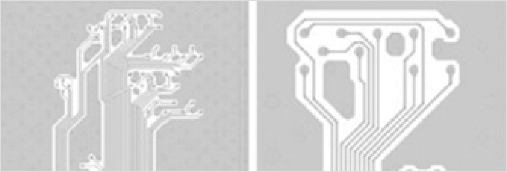
- ・Masks for IC bump packaging
- ・Masks for Semiconductor Packaging Substrates
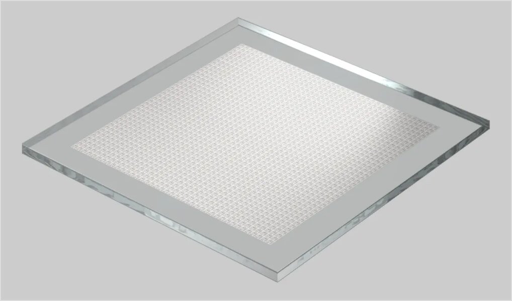
- ・Masks for Micro Lens Array
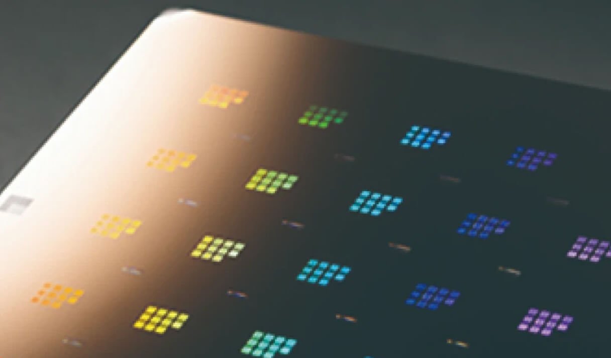
- ・Masks for LED
- ・Masks for Thermal Head
- ・Masks for Tool Accuracy Control
- ・Test masks for OEM qualification and research
- ・Master masks for High-resolution Printing
- ・Masks for various R&D applications
- ・Please contact Tekscend for more information.
Specification Outline
-
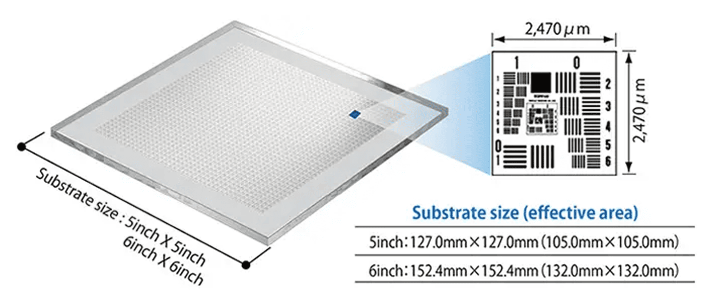
Mask Size 4 inch, 5 inch, 6 inch, 7 inch and 9 inch formats of various thickness. Wafer Size 200mm
Please contact us about other sizes. -
Acceptable Data Format GDS, GBR, or Design diagram
-
Substrate types: Synthetic Quartz, Soda-lime Glass / Thickness: 0.09~0.25 inch (t)
Pellicle mounting possible
Tekscend Test Pattern Photomasks
Tekscend Test pattern photomask form the basic-shaped pattern with chromium on the high purity glass substrate.
Such photomasks are used for accuracy management of equipment, resolution checks, and evaluation of photoresist selection.
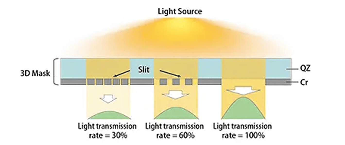
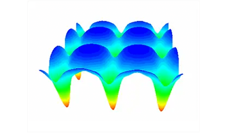
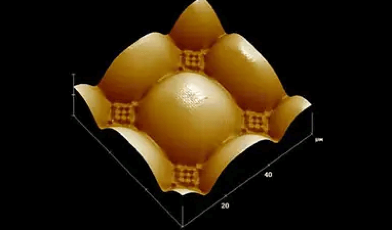
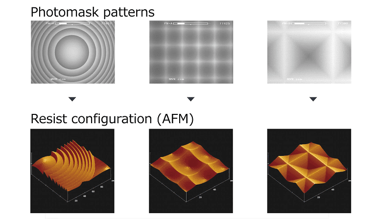
3D Photomasks
3D Mask (gray-scale mask, gray-tone mask) is a 3D photomask, applying the well-established photomask technology creating variable transmission of light across the photomask in order to facilitate creation of 3D structures.