About Molds for Nanoimprinting
Nanoimprinting is a microfabrication technology that transfers patterns at the tens of nanometer level by pressing a mold, which serves as an original plate. Because of the simplicity of the process, nanoimprinting is expected to be a technology for mass production of microstructures at low cost and with good reproducibility.
Nanoimprinting Methods and Types of Molds
Methods of Nanoimprint Lithography
Nanoimprint lithography can be classified into two types: "UV Method" and "Thermal Method"
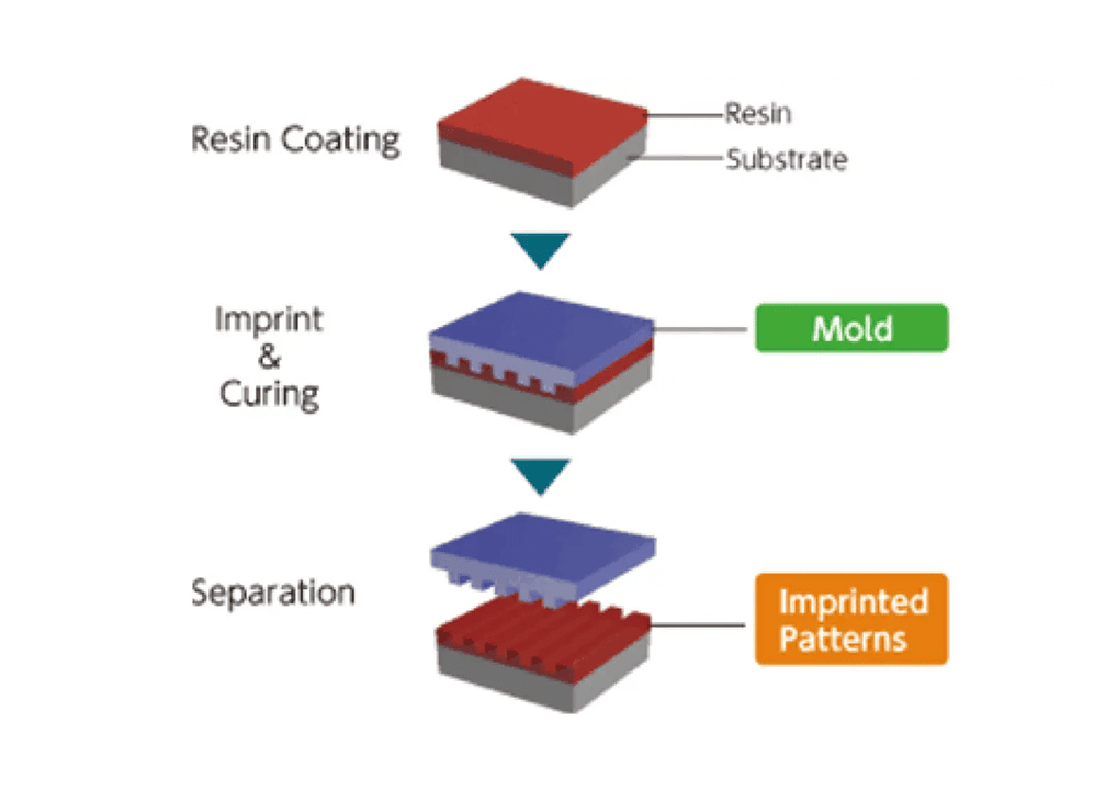
UV Nanoimprint Method
The UV nanoimprint method replicates patterns by pressing a patterned mold against UV-curable resin, which is then hardened by UV irradiation. This process works at normal temperature, giving this method the unique nature of allowing a high level of precision in the replication of patterns.
Thermal Nanoimprint Method
The thermal nanoimprint method replicates patterns by pressing a patterned mold strongly against a thermoplastic resin, which is then cooled after being heated. Direct processing is possible for a variety of products if they are made of materials that are softened by heating.
Mold Types
Quartz Molds
This quartz mold is primarily used in the UV nanoimprint process.Tekscend Photomask's quartz molds are made of high-quality quartz substrate equivalent to that used for semiconductor photomasks, and have excellent stability and flatness. By applying the semiconductor photomask manufacturing process, our molds are capable of producing high-resolution patterns in the tens of nanometers. We also develop and manufacture molds with multi-step structures to meet a wide range of needs. Substrate size: 152 x 152 x 6.35 mm (t)
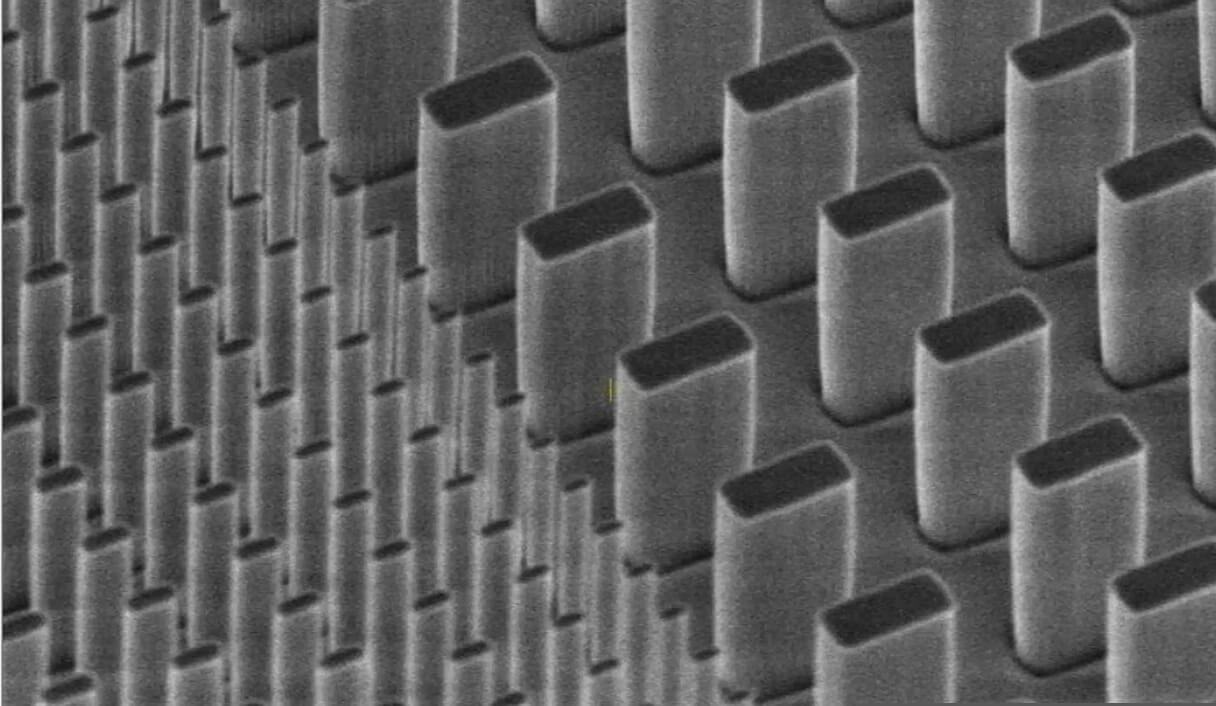
Silicon Molds
This silicon mold is primarily used in thermal nanoimprinting processes.Tekscend Photomask's silicon molds are manufactured by drawing a precise pattern on a photosensitive resist coated on a silicon substrate using an electron beam, and then deep drawing the pattern using a dry etching method. This process achieves the same high precision as quartz mold manufacturing and enables the production of silicon molds with high aspect ratio patterns and complex 3D shapes. Substrate size: 200 mm diameter (wafer thickness: 725 μm)
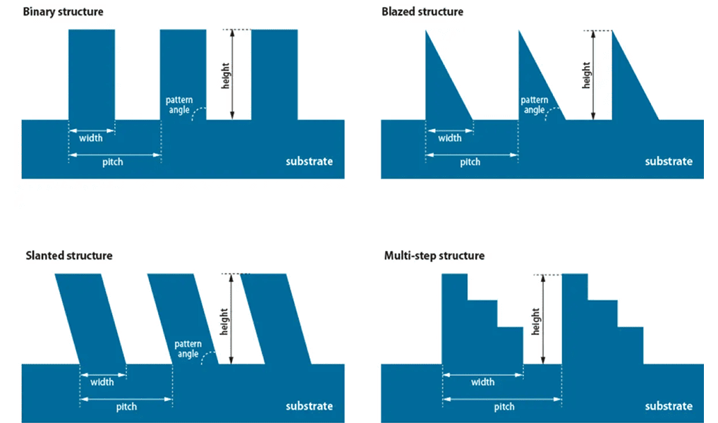
Pattern Shape Examples
Tekscend has had extensive achievements offering various molds to satisfying customers' needs. We are also focusing on research and development, including three-dimensional structure patterns.
Please feel free to consult us regarding your desired pattern shape, etc.