About Photomask
A photomask is a glass plate having a light shielding film on which ultra fine circuit patterns are formed, and used to produce patterns of complicated semiconductor circuits onto silicon wafers. In addition to products for semiconductors, we develop and manufacture glass masks for various studies and development, silicon stencil masks, molds for nanoimprinting, etc.
Products
Photomasks for Semiconductors
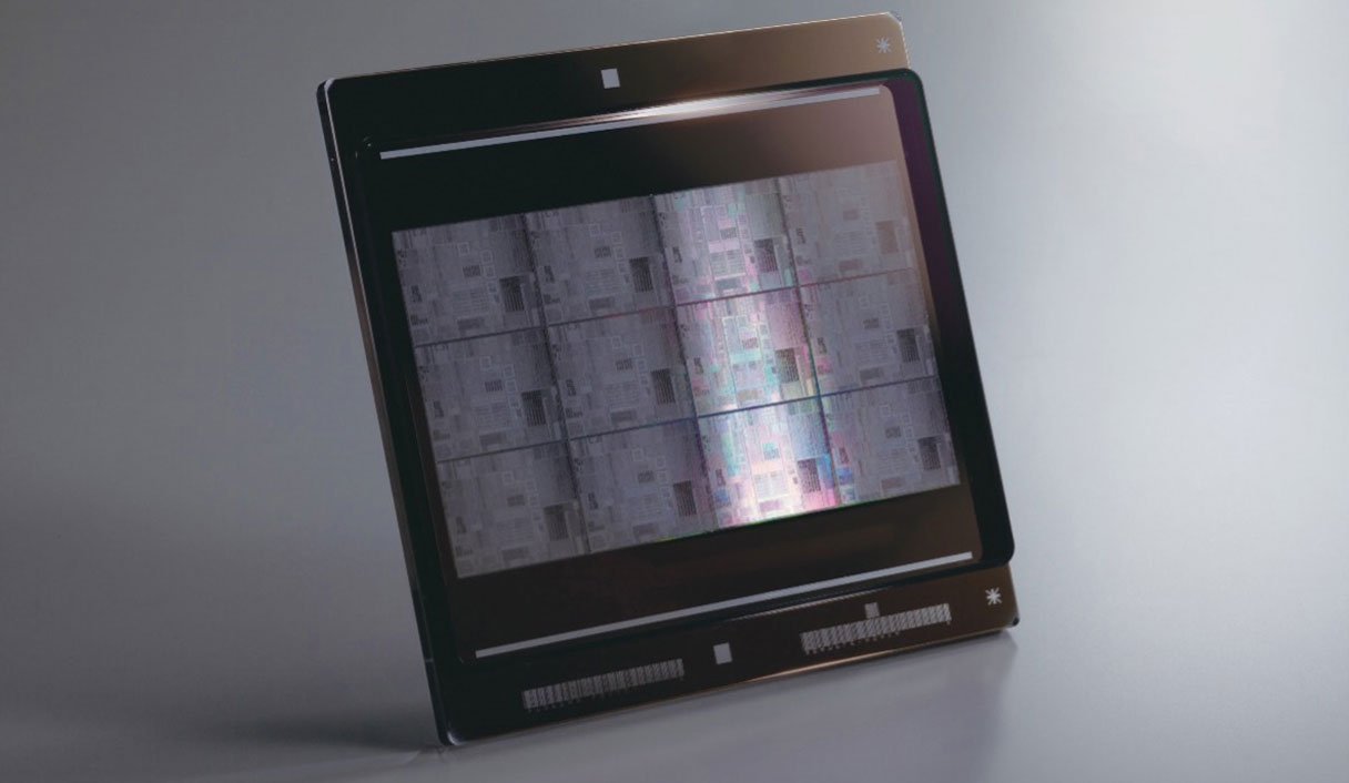
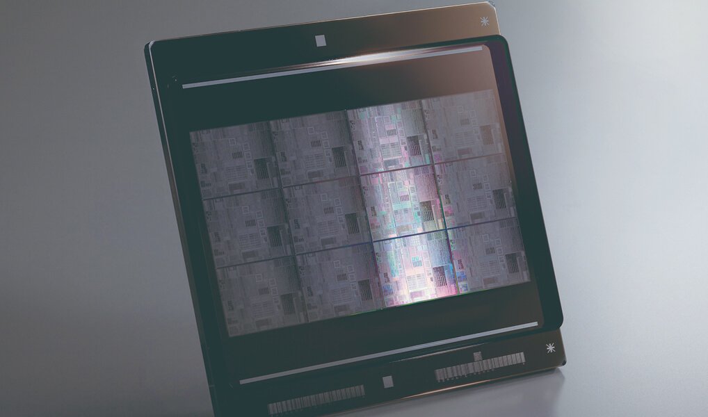
Photomasks play an important role in the semiconductor manufacturing process and are the master plates used to transfer circuits onto semiconductor wafers. Based on circuit data, an electron beam is used to create an electronic circuit pattern on a photomask substrate (mask blank), which is then etched with chemicals, stripped of photoresist (photosensitive material), cleaned, measured, and inspected before the photomask is completed.
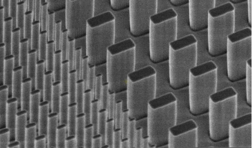
Molds for Nanoimprint
Nanoimprinting is a microfabrication technology that transfers patterns at the tens of nanometer level by pressing a mold, which serves as an original plate. Because of the simplicity of the process, nanoimprinting is expected to be a technology for mass production of microstructures at low cost and with good reproducibility.
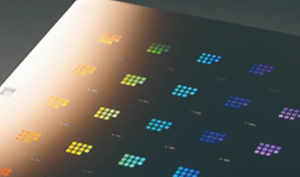
Photomasks for Various Applications
Tekscend Photomask provides high resolution, highly reliable photomasks not only for semiconductors, but also for different industrial areas and research purposes, utilizing its microfabrication technology.