Details on Toppan Printing's Next-Generation EUV Photomask
Toppan Printing Co., Ltd. (hereafter Toppan Printing; head office: Chiyoda Ward, Tokyo; President & Representative Director: Shingo Kaneko) has developed a next-generation EUV photomask for leading-edge semiconductors. The new photomask minimizes the unwanted reflection of light to peripheral sections during EUV exposure,*1 a next-generation semiconductor manufacturing technology.
Sample shipments to semiconductor manufacturers will begin in fiscal 2016, with the start of full-scale mass production slated for fiscal 2017. Based on this technology, Toppan Printing is aiming to establish the industry standard for next-generation EUV photomasks. This development marks the first time anywhere in the world that a structure to suppress the unwanted reflection of light to peripheral sections has been created on the surface of an EUV photomask, and the areas around the pattern have been miniaturized.
A presentation on the new technology will be made at the SPIE Advanced Lithography 2016 international conference, held at the San Jose Convention Center in San Jose, California, U.S.A. from February 22 to 25, 2016.
■ Background
With growing demand for semiconductors with even higher performance for applications such as big data analysis, artificial intelligence, and the commercialization of driverless car technology, EUV exposure is garnering attention as a next-generation semiconductor manufacturing technology. Practical application of the technology will enable further miniaturization of semiconductors and the manufacture of processers that are smaller, faster, and require less power than current models.
EUV exposure-based semiconductor manufacturing involves light from a particular source being reflected by the EUV photomask to form a pattern on a silicon substrate. In addition to the EUV light needed for patterning, this light also contains various wavelengths that are not required, known as out-of-band (OOB) light. This OOB light has adversely affected the accuracy of formation of sections periphery to the pattern on silicon substrates.
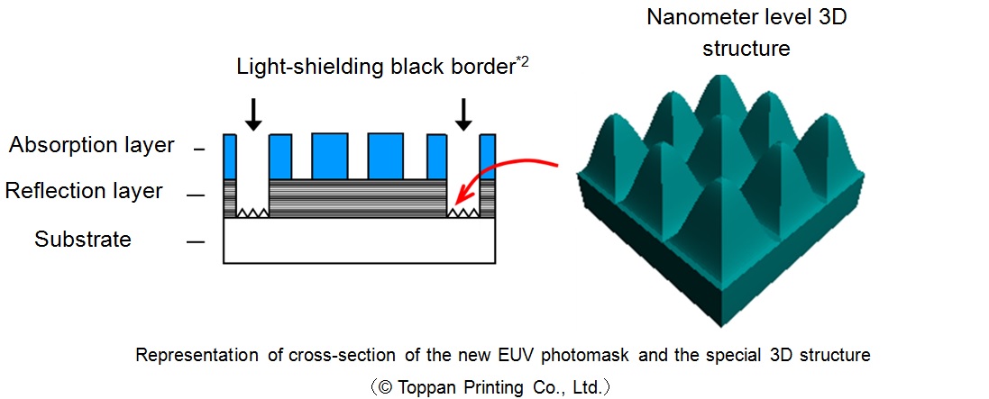
To overcome this, Toppan Printing has improved a section called the light-shielding black border. This is located on the periphery of an EUV photomask pattern and suppresses the unwanted reflection of EUV light. Toppan Printing has further advanced and combined its microfabrication and optical design technologies to develop a next-generation EUV photomask with a special three-dimensional structure on the light-shielding black border of the mask, enabling better control of light from the light source.
Toppan Printing is one of the world’s leading photomask producers. By supplying advanced photomasks, it provides extensive support to semiconductor manufacturers’ operations, from the launch of leading-edge processes to subsequent mass production. Toppan developed the conventional EUV photomask that has become the industry standard in 2012 and has successfully developed the new next-generation mask based on further miniaturization. Through ongoing R&D activities, Toppan Printing intends to continue contributing to the evolution of semiconductor manufacturing technology.
■ Features: Special 3D structure that suppresses the reflection of light and improves yield
By further developing and fusing its microfabrication and optical design technologies, Toppan Printing has become the first company in the world to form a special 3D structure on the light-shielding black border on the surface of an EUV photomask and reduce the reflection of OOB light by approximately 70% compared with conventional products. Transfer testing using EUV exposure machinery manufactured by ASML*3 has verified that this new EUV photomask can reduce dimension variability on silicon substrates by two-thirds. As a result, it enables improvements in quality and yield for semiconductor patterns.Comparison of reflectance of conventional and next-generation EUV photomasks
(light-shielding black border)
|
Mask type |
EUV light reflectance |
OOB light reflectance |
|
Conventional EUV photomask |
Less than 0.05% |
5-6% |
|
Next-generation EUV photomask |
Less than 0.05% |
1.5% or less |
■ Future targets
Toppan Printing will begin sample shipments to its global semiconductor manufacturing clients during fiscal 2016. We will also further advance development, targeting commercialization and establishment as the industry standard from 2017, when mass production is scheduled to begin.
*1 EUV exposure: An exposure technology for transferring a semiconductor circuit pattern to a silicon substrate. It uses extreme ultraviolet light with a wavelength of 13.5 nanometers (1 nanometer=1 billionth of a meter).
*2 Light-shielding black border: Area located on the periphery of an EUV photomask pattern in which the unwanted reflection of EUV light is suppressed.
*3 ASML: Headquartered in the Netherlands, ASML is the world’s only manufacturer of EUV exposure machinery for semiconductor manufacture.
*Patents are pending for the technologies described in this press release.
*The names of companies, products, and services featured in this press release are the trademarks or registered trademarks of the respective companies.
*The information in this press release is current as of the date of publication and is subject to change without notice.